产品详情
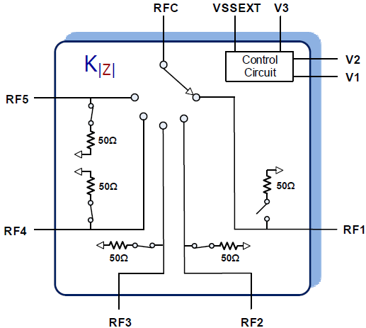
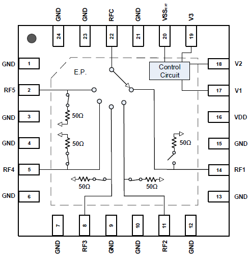
- 五个对称宽带、吸收式射频端口
- 恒定阻抗,Kz,特性
- 高性能射频
- 2700MHz 时隔离度为 50dB
- 2700MHz 时插入损耗为 1.2dB
- 高连续射频连续功率处理能力
- 所选射频路径:33dBm
- 终止射频路径:27dBm
- 高线性度:
- IIP2 为 114dBm
- IIP3 为 60dBm
- 2.7V 至 5.50V 单电源电压
- 外部负电源选项
- 3.3V 和 1.8V 兼容控制逻辑
- 工作温度 -40 °C 至 +105 °C
- 4mm x 4mm 24 引脚 QFN 封装
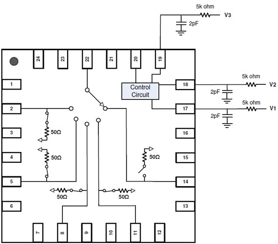
F2915是一款高可靠性、低插入损耗、50? SP5T 吸收式射频开关专为各种无线和其他射频应用而设计。该器件覆盖从 50MHz 到 8000MHz 的宽频率范围。除了提供低插入损耗外,F2915 还提供出色的线性度和隔离性能,同时提供 50?终止未使用的射频端口。 F2915 还包括正在申请专利的恒定阻抗 (Kz) 功能。 Kz 提高了热开关耐用性,最大限度地减少了 VCO 中的 LO 牵引,并减少了配电网络中的相位和幅度变化。它还非常适合在两个或多个放大器之间进行动态切换/选择,同时避免损坏 PA 和 ADC 等上下游敏感器件。
F2915 使用单个正电源电压,支持使用 3.3V 或 1.8V 控制逻辑的三个逻辑控制引脚。将负电压连接到引脚 20 会禁用内部负电压发生器并成为负电源。
产品文档
类型
姓名
日期
动作
2025-08-25
F2915 产品简介 REVA
2025-08-25
射频开关 Family
2025-08-25
F2915 数据表
2025-08-25
PCN# : Q1703-01 Die Revision Change| F2915NBGK
2025-08-25
PCN# : A1809-04 Add Alternate Assembly 地点 for QFN 包裹s
2025-08-25
F2915 S-parameters
2025-08-25
F2915 IBIS Model
2025-08-25
PCN# : 210003 Add Alternate Fab 地点 on 选择 RFD Devices
Boards and Kits
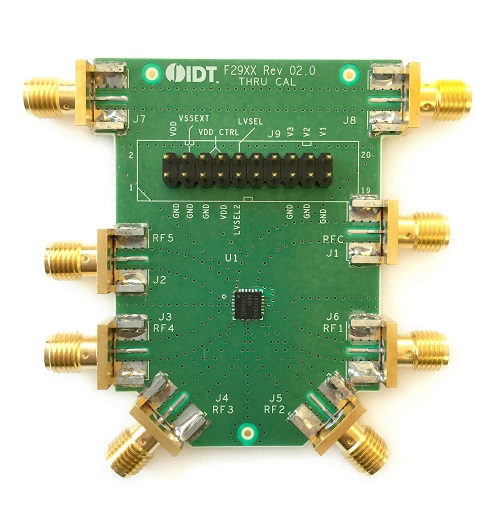
Evaluation Board for 高 Reliability SP5T Absorptive RF Switch
The F2915EVBI is a fully populated evaluation board which allows the customer to easily evaluate the F2915 RF switch.
“Thru” calibration connectors are conveniently located on the eval board to simplify the calibration process prior to making any RF measurements. Each RF port (RF1, RF2, RF3, RF4 and RF5) can be connected to RFC by 申请ing the correct control logic voltage to the V1, V2 and V3 control pins as outlined in the F2915 数据表. The Vssext feature gives the customer the option to supply an external negative voltage to the Vssext header pin to shut down the internal charge pump for low spur operation.
部件号 (2)
F2915NBGK8
F2915NBGK
您还有其他问题吗?
我们致力于帮助您探索各种可能性,优化性能,并推动技术进步。立即联系我们!
与销售人员交谈