产品详情
- 双对称宽带、吸收式射频端口
- 2GHz 高性能射频
- RFC-RFX 隔离度为 67dB
- 插入损耗为 0.79dB
- 高连续射频连续波功率处理能力
- 所选射频路径:34dBm
- 终止射频路径:27dBm
- 高线性度:
- IIP2 为 111dBm
- IIP3 为 64dBm
- 3.3V 和 1.8V 兼容控制逻辑
- 工作温度为 -40 °C 至 +105 °C
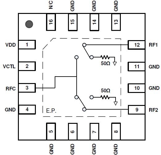
- 4mm x 4mm 16 引脚 QFN 封装
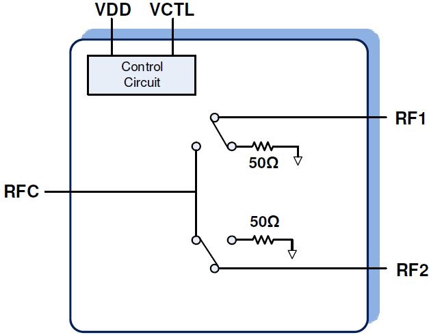
F2933是一款高可靠性、低插入损耗的产品,50?单刀双掷 (SP2T) 吸收式射频开关,专为广泛的市场和应用而设计。该器件覆盖 50MHz 至 8000MHz 的宽频率范围,工作温度范围为 -40°C 至 105°C,电源电压范围为 2.7V 至 5.5V。 F2933 专为高功率处理而设计,P1 dB 高达 36.5dBm,支持直通路径中 34dBm 的峰值工作功率以及端接 RF 端口中 27dBm 的热开关功率。除了提供低插入损耗外,F2933 还提供高隔离度和低失真性能,同时提供 50?端接至未使用的 RF 端口。
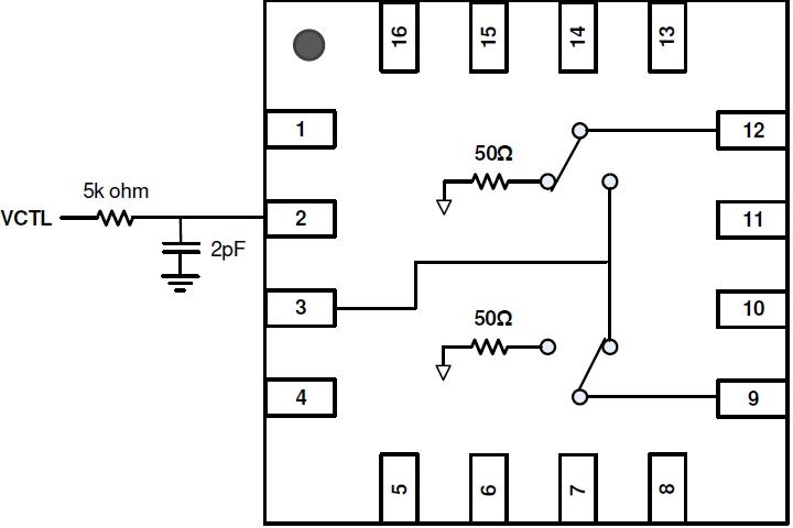
F2933 使用单个正电源电压,支持使用 3.3V 或 1.8V 控制逻辑的三个逻辑控制引脚。
Boards and Kits
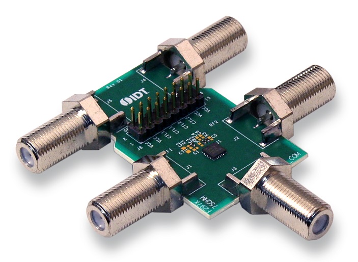
Evaluation Board for 高 Reliability SPDT Absorptive RF Switch
The F2970EVBI is a fully populated, enabling easy RF evaluation of the product.
“Thru” calibration connectors are conveniently located on the eval board to simplify the calibration process prior to making any RF measurements. The RF through measurement (RF1 to RF2) can be made by 申请ing the correct control logic voltage to the control pins as outlined in the 数据表. DC power, ground and the control voltages are applied to the pin header.
部件号 (3)
F2933NBGP8
F2933NBGP
F2933EVBI
您还有其他问题吗?
我们致力于帮助您探索各种可能性,优化性能,并推动技术进步。立即联系我们!
与销售人员交谈